Scanning Tunneling (STM) and Atomic Force (AFM) Microscopes
The Scanning Tunneling Microscope
This device, which led to a Nobel Prize in Physics, is based on the tunneling current experienced by approaching the electronic cloud surrounding an atom on a surface by a single atom pointed probe[1]. The probe is silicon and carries a small voltage with respect to a substrate. When the electronic wave functions, or orbitals, of the tip atom and the substrate atoms overlap, there is a small detectable current flow; this current has to burrow through a resistive barrier (since true “contact” is not made) by a process known as “tunneling”. The applied potential is insufficient to actually jump the insulating barrier (in classical terms), but the current has a quantum mechanical ability to tunnel through the resistive barrier.
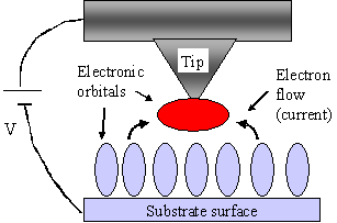
In the simplest quantum mechanical view, the probability of tunneling is exp(-E/V) where E is the classical energy to jump the insulation barrier and V is the actual potential difference that is applied. This has a finite value even when V < E and is larger (i.e., more current) when V is larger or E is smaller. By carefully monitoring the tunneling current, a map of the surface electronic structure is formed.
The Atomic Force Microscope
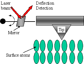
This is a similar instrument to the STM and indeed uses the same basic hardware but the principle of operation is different. The tip is moved into “contact” with the surface atoms; the tip is connected to a cantilever beam to which is attached a tiny mirror. An incident laser beam is bounced off the mirror and, using a sophisticated analysis and detection scheme, the motion of the tip is inferred and plotted as a 2- or 3-dimensional image.
The image of “IBM” spelled in xenon atoms was a technological tour-de-force; it was made with an AFM by using its tip to move individual atoms. The tendency of the atoms to move due to thermal energy was greatly reduced by conducting the experiment at the temperature of liquid helium (about 4 K).
The Eigler & Schweizer Experiment

To spell out “IBM” with 35 individual Xe atoms one must: a) have a clean flat tablet on which to write, b) make sure that the atoms do not move, c) make sure the atoms are large enough to read and d) make sure the atoms do not react with the substrate.
An atomically clean single crystal face of a piece of nickel provided the tablet; ultra low pressures in a vacuum chamber precluded impurities accumulating from the vapor phase, and a low temperature of just 4 K reduced the vibratory and translational motions on the surface. Finally, if you consult your periodic table, you will see that the sizes of the atoms increase with each row as additional principal quantum levels are added (i.e., reading down the rows for a fixed column). The unreactive noble gas xenon atoms have a relatively large atomic diameter of 0.25 nm and can be read against the smooth nickel crystal background.
What kind of instrument is used to move the atoms into such precise positions? It is an electrochemically-etched cantilever probe used on a STM; with specialized techniques, the tip diameter can be reduced to that of a single atom (for Si this is about 0.3 nm, i.e., comparable to that of the Xe atoms). This achievement itself is a technological tour-de-force.
Footnotes and References
[1]. http://physics.nist.gov/GenInt/STM/text.html
Contact: koskyp@union.edu
Self-Assembly from Condensed Phases | Department of Physics & Astronomy | Union College Home Page
Self-Assembly from the Gas Phase by Bottom-Up Technology © 2003 Kosky.
Last Updated: 08/05/05 01:10 PM