Molecular Beam Epitaxy
MBE was introduced by Cho & Arthur[1] in the late 1960s and early 1970s as a means of growing high-purity epitaxial layers of compound semiconductors. By ”epitaxial” it is meant that new layers of a crystalline compound, as deposited by chemical reactions from the gaseous molecules in the beam, will perfectly align with the original crystal that acts as the target or substrate. Quoting from this web article, “MBE can produce high-quality layers with very abrupt interfaces and good control of thickness, doping, and composition. Because of the high degree of control possible with MBE, it is a valuable tool in the development of sophisticated electronic and optoelectronic devices”.
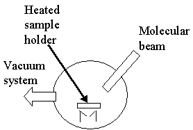
MBE is a true early application of nano self-assembly since the technique relies on an atom-by-atom building of the epitaxial structures. As such it was, and is, an inherently a laborious process. The attached sketch gives a highly simplified physical description. A (molecular) beam of reactive molecules is ballistically “fired” at a surface of a substrate on which there is a small crystal of a material that will react with the molecules in the beam.
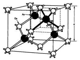
Typically, the substrate target is a semiconductor material with useful electronic properties. The molecular beam quite often is composed of evaporated elemental substances such as gallium and arsenic (GaAs, or gallium arsenide, is one of an important class of high temperature semiconductors used in the electronics industry); the crystalline structure of GaAs can be represented as per the inset[2]. The dark spheres represent the location of arsenic atoms and the light ones the gallium. In reality electronic orbitals of the atoms fill almost all of the space in the crystal. By carefully controlling the beams of Ga and As vapors, this structure is replicated atom-by-atom. It requires a very good vacuum of 10-4 Pa or better so that the beams are not scattered out of their intended pathway by background gas in the chamber.

Epitaxy is called “homoepitaxy” if the depositing materials are identical to the target material (as shown in the upper sketch, the deposition substrate is the same material as we are depositing from the beam). What we are doing is to make more of the target material in exactly the same crystalline structure as the target material.
In “heteroepitaxy” the substrate is a different chemical species to the depositing beam but has a crystalline structure that geometrically mimics a new material crystal that now can be deposited on the target. For example, the GaAs “seed” crystal is used to replicate another material of the same geometry as GaAs, but chemically different from it. Whether one succeeds depends specifically on the closeness of the match of the crystal faces of the deposited material to those of the seed substrate.
One well-known example of heteroepitaxy is called by a mnemonic “SOS” for “silicon-on-sapphire”. In this technique, silicon is bonded via MBE onto a substrate of crystalline Al2O3 (i.e., sapphire). It is used for a variety of electronic purposes (you can try searching SOS/sapphire/Si on Google for many commercial suppliers of the product).
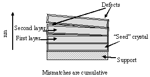
The requirements of heteroepitaxy are more rigorous than for homoepitaxy since it is difficult to exactly match one crystalline material to another; defects tend to build with multiple layers as per the inset simplified sketch.
An attached photograph and schematic shows that MBE is a complicated technique. A practical MBE unit has features for shuttering the beams as well as manipulating the target. Thus the beams are typically produced in shuttered effusion cells (which are small hot ovens with pinhole outlets). These beams are “fired” at the target in specified sequences; the moveable target is heated and the background surfaces areas are cooled. Finally, and not least, are in situ diagnostic devices (the particular one displayed in the schematic is called RHEED, reflection-high energy electron diffraction). There are several other sophisticated diagnostic devices that are also used.
Consider the physical requirements for MBE: 1) one or more molecular beams that interact only with the target substrate and not with each other while in transit from the source of the beams, 2) an atomically clean surfaces on which to grow and 3) a defect-free crystalline deposit. Much of the reason for the complicated apparatus can be readily adduced from principles that we have already learned. The gas laws strongly influence the first two of these criteria and what we have learned about chemical bonding will influence both items 2 and 3.
Footnotes and References
[2]. http://www-ncce.ceg.uiuc.edu/tutorials/crystal_structures/gaas.html
Contact: koskyp@union.edu
Self-Assembly from the Gas Phase by Bottom-Up Technology | Department of Physics & Astronomy | Union College Home Page
Self-Assembly from the Gas Phase by Bottom-Up Technology © 2003 Kosky.
Last Updated: 08/05/05 10:43 AM